About the Company:
A leading supplier of equipment and process solutions for the manufacture of semiconductors, and microelectromechanical systems (MEMS), compound semiconductors, power devices and nanotechnology devices.
Challenge:
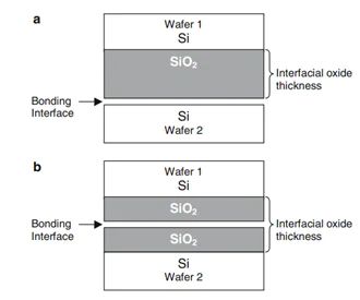
Wafer direct bonding is a critical technique essential for the MEMS packaging. O2 plasma appears to be a very attractive alternative to conventional wet treatments for prebonding surface activation. The schematic of wafer bonding of sandwich-like structures, Si/SiO2 or SiO2/ SiO2 is shown in figure.

Figure 1 Schematic illustration of the sandwich-like structures: (a) Si/SiO2 or (b) SiO2/SiO2 wafer bonding
In order to successfully bond two wafers, the surfaces must first be prepared. This usually requires wafer tests to qualify the tool performance for modifying the surface, which results in a process that runs for a fixed amount of time. Normal chamber drift affects this time, so re-qualification needs to happen often, which impacts tool throughput. Wafer bonding is also quite late in a wafer fabrication cycle, so scrappage is very costly.
Our Innovation:
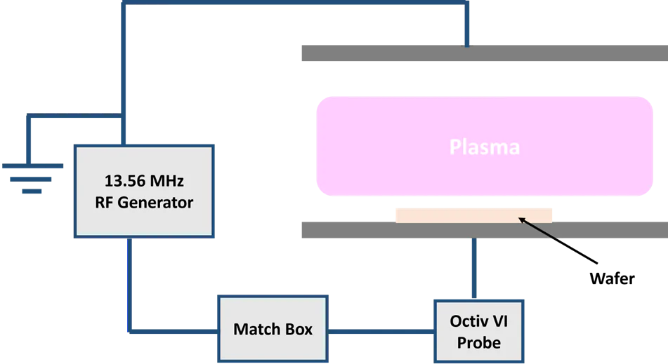
An external sensor, the Octiv Poly VI probe was used to monitor the wafer directly and determine when surface treatment was complete. The sensor, mounted after the match box, required precise accuracy in non-50 Ohm environments due to the plasma impedance being near 1 kOhm in magnitude.

Figure 2 Schematic of plasma chamber (CCP chamber) with an Octiv installed post-match on the bottom electrode.
Sensor-to-sensor repeatability was crucial to ensure consistent tool performance across different chambers, without the need for tool-to-tool adjustments. The application needed to deliver identical performance on every chamber module.

Figure 3 Growth of Silicon Oxide layer on Si wafer
The Solution:
The final model leveraged the Octiv’s precise current measurements to monitor oxide layer growth with 0.5 Angstrom precision. This allowed the tool to accurately detect when the process was complete, improving throughput by eliminating the need for process qualification steps. Scrappage was also eliminated, as the sensor’s feedback naturally adjusted process time to compensate for tool drift.
The integration was achieved using the industry-standard EtherCAT protocol.
Additional verifications of this technique were completed using the Quantum RFEA. The sensor provides real time measurements of ion energy, ion flux and ion to neutral ratio reaching over the wafer during plasma process. This helped to understand the full bonding and growth process.
To download the case study click here.
To learn more about our plasma measurement products contact us at [email protected]